Design
The input current is offset by a negative feedback current flowing in the capacitor, which is generated by an increase in output voltage of the amplifier. The output voltage is therefore dependent on the value of input current it has to offset and the inverse of the value of the feedback capacitor. The greater the capacitor value, the less output voltage has to be generated to produce a particular feedback current flow.
The input capacitance of the circuit is almost zero because of the Miller effect. This ensures that the stray capacitances (the cable capacitance, the amplifier input capacitance, etc.) are virtually grounded and have no influence on the output signal.[1]
Ideal circuit
This circuit operates by passing a current that charges or discharges the capacitor  during the time under consideration, which strives to retain the virtual ground condition at the input by off-setting the effect of the input current:

Referring to the above diagram, if the op-amp is assumed to be ideal, then the voltage at the inverting (-) input is held equal to the voltage at the non-inverting (+) input as a virtual ground. The input voltage passes a current  through the resistor producing a compensating current flow through the series capacitor to maintain the virtual ground. This charges or discharges the capacitor over time. Because the resistor and capacitor are connected to a virtual ground, the input current does not vary with capacitor charge, so a linear integration that works across all frequencies is achieved (unlike RC circuit § Integrator).
The circuit can be analyzed by applying Kirchhoff's current law at the inverting input:

For an ideal op-amp,  amps, so:

Furthermore, the capacitor has a voltage-current relationship governed by the equation:

Substituting the appropriate variables:

For an ideal op-amp,  volts, so:

Integrating both sides with respect to time:

If the initial value of  is assumed to be 0 volts, the output voltage will simply be proportional to the integral of the input voltage:[2]

Practical circuit
This practical integrator attempts to address a number of flaws of the ideal integrator circuit:
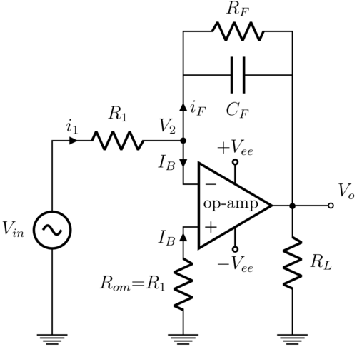
Real op-amps have a finite open-loop gain, an input offset voltage  and input bias currents
  , which may not be well-matched and may be distinguished as
  going into the inverting input and
  going into the non-inverting input. This can cause several issues for the ideal design; most importantly, if
  , both the output offset voltage and the input bias current can cause current to pass through the capacitor, causing the output voltage to drift over time until the op-amp saturates. Similarly, if
  were a signal centered about zero volts (i.e. without a DC component), no drift would be expected in an ideal circuit, but may occur in a real circuit.
To negate the effect of the input bias current, it is necessary for the non-inverting terminal to include a resistor  which simplifies to
  provided that is much smaller than the load resistance
  and the feedback resistance
  . Well-matched input bias currents then cause the same voltage drop of
  at both the inverting and non-inverting terminals, to effectively cancel out the effect of bias current at those inputs. A CMOS op amp should be selected to minimize errors from input bias current,[3] since MOSFET gates don't require DC current and only have small leakage current on the order of picoamps (pA).[4]
Also, in a DC steady state, an ideal capacitor acts as an open circuit. The DC gain of the ideal circuit is therefore infinite (or in practice, the open-loop gain of a non-ideal op-amp). Any DC (or very low frequency) component may then cause the op amp output to drift into saturation.[5] To prevent this, the DC gain can be limited to a finite value by inserting a large resistor  in parallel with the feedback capacitor. Note that some op amps have a large internal feedback resistor, and many real capacitors have leakage that is effectively a large feedback resistor.[6]
The addition of these resistors turns the output drift into a finite, preferably small, DC error voltage:

There are other methods, which may be combined, to deal with offset error. A variation of this circuit simply uses an adjustable voltage source instead of  and some op amps with very low offset voltage may not even require offset correction.[3] Offset correction is a bigger concern for older op amps, particularly BJT types. Another variation circuit to avoid offset correction that works for AC signals only is to capacitively-couple the input with a large input capacitor before which will naturally charge up to the offset voltage. Additionally, because offset may drift over time and temperature, some op amps provide null offset pins, which can be connected to a potentiometer whose wiper connects to the negative supply to allow readjusting when conditions change.[6] It should also be noted that the integrator is commonly used as part of a feedback/servo loop which provides the DC feedback path, removing the need for a feedback resistor.[3]
Frequency response
Both the ideal and practical integrator have a gain of 1 at a single frequency called the unity gain frequency  :
:

But the overall frequency response of the two circuits differ due to their different pole locations.


